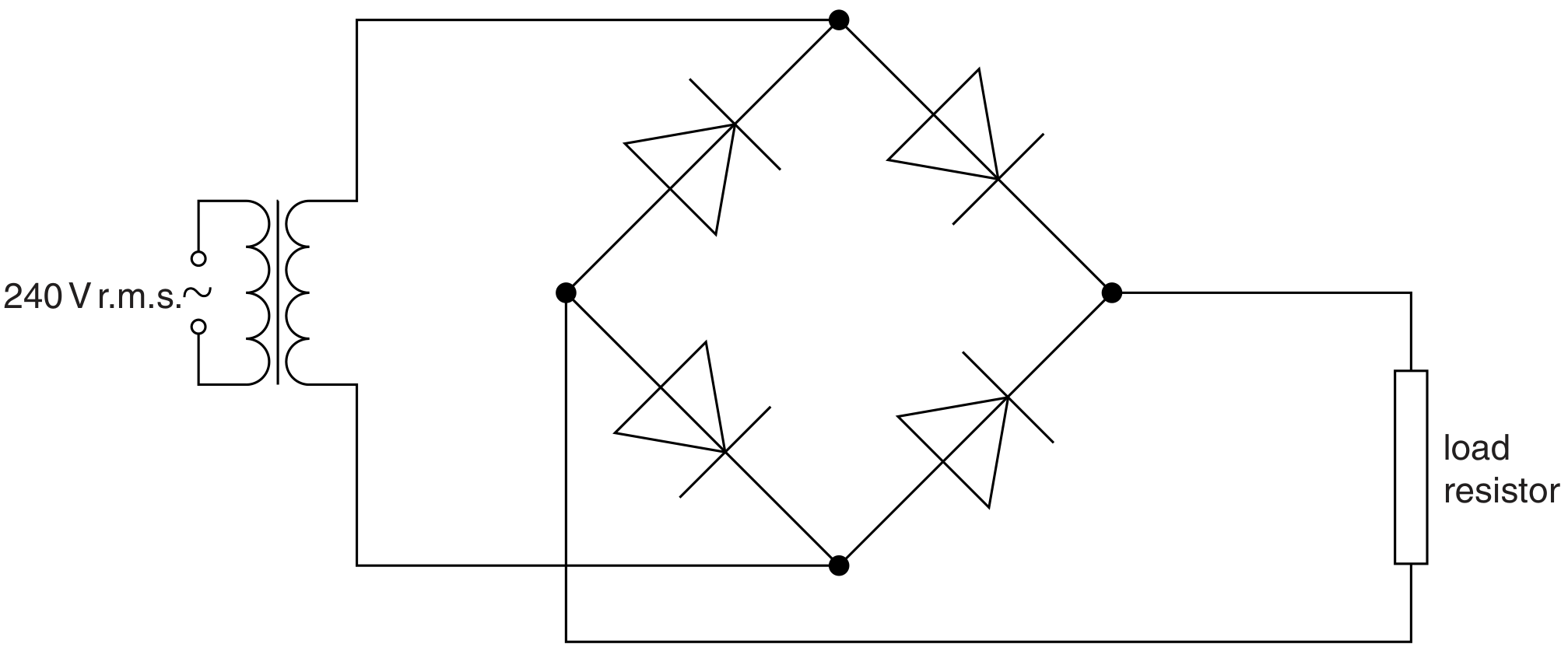
EduNinja
(a)

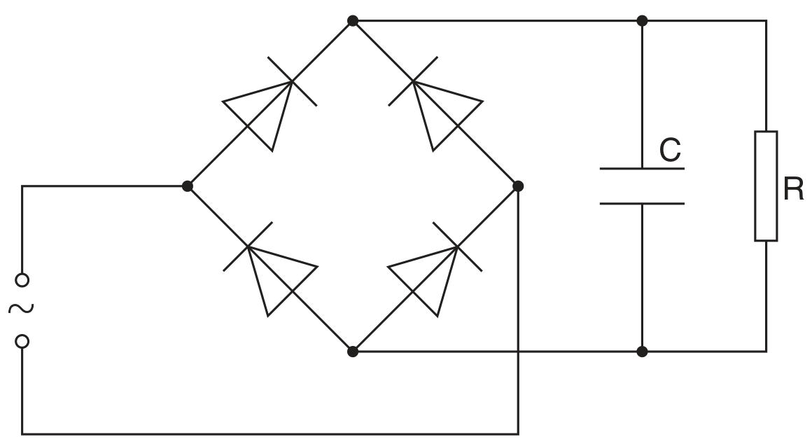
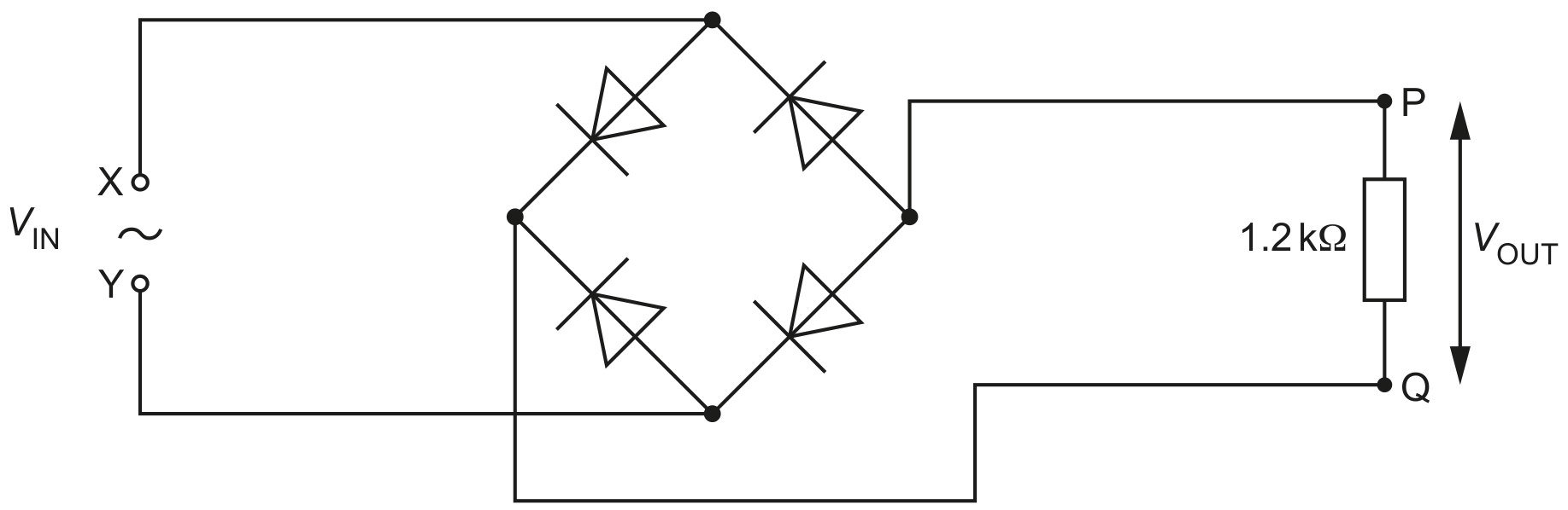
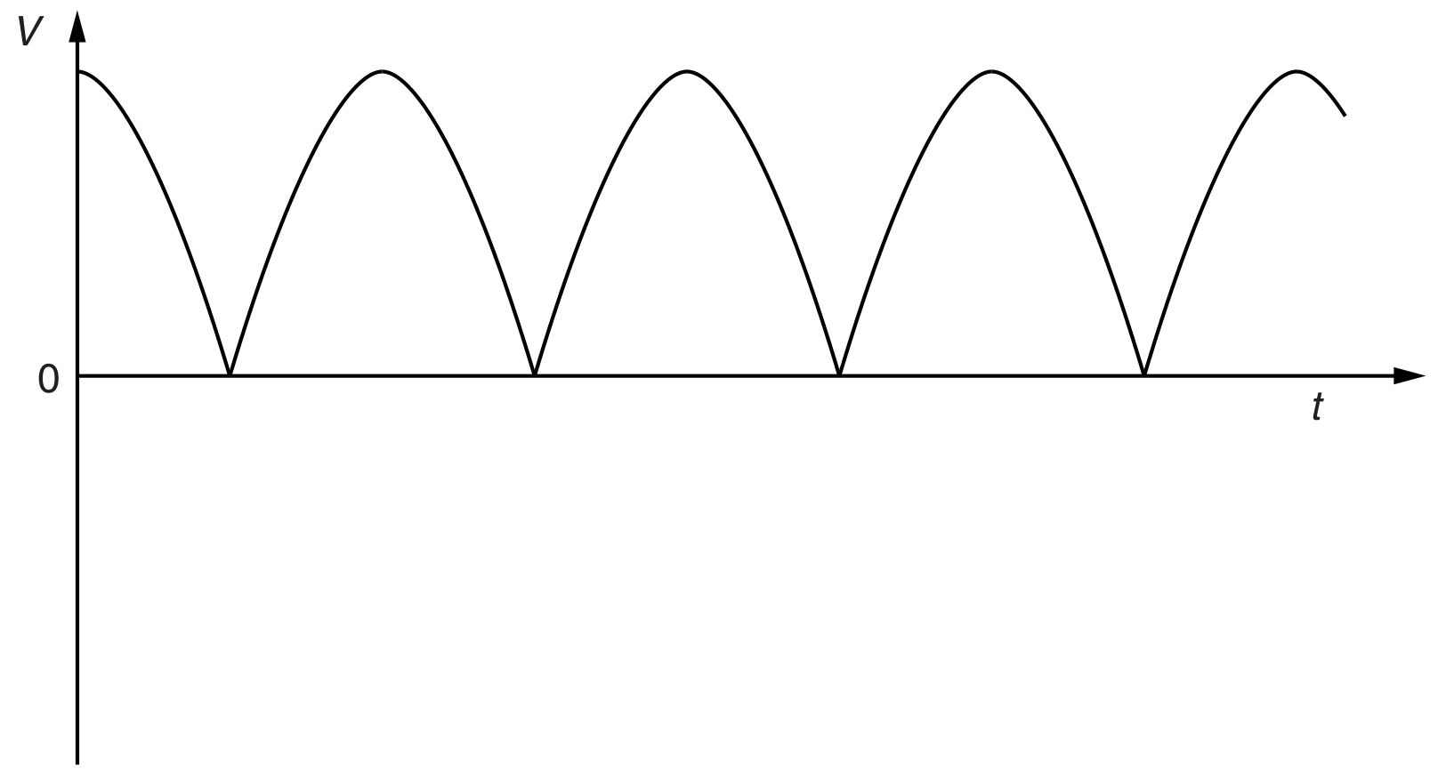
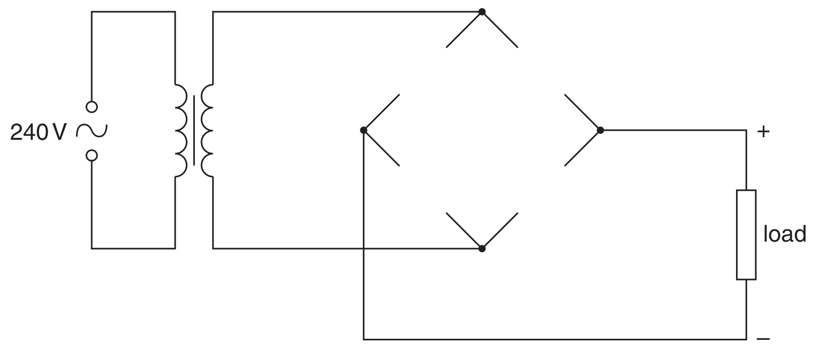
A sinusoidal a.c. power supply is connected to the input of a bridge rectifier. The output of the rectifier is connected to a load resistor.

[ 4 ]
(i)

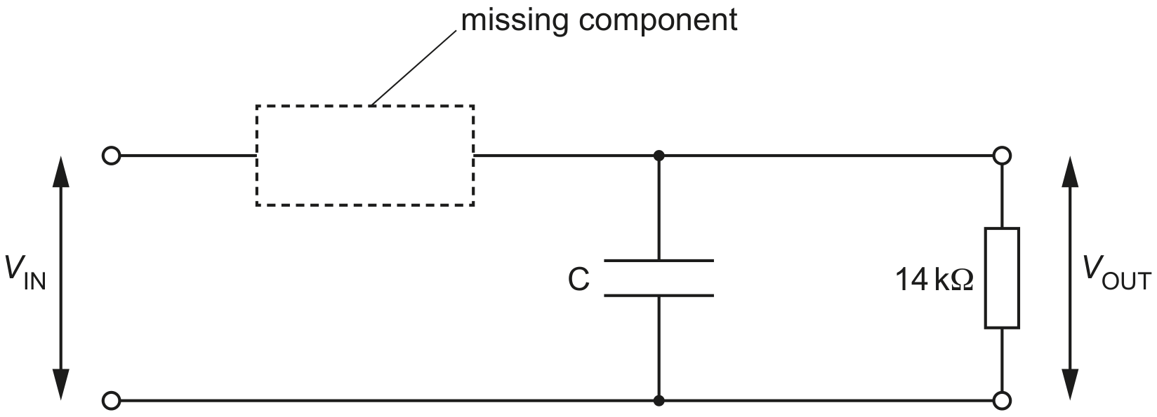
Complete the circuit in Fig. 4.2 by adding a capacitor to smooth the p.d. across the load resistor.
connections from output of bridge rectifier
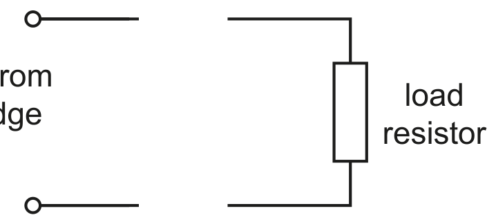
Fig. 4.2

Fig. 4.2

[ 1 ]
(ii)

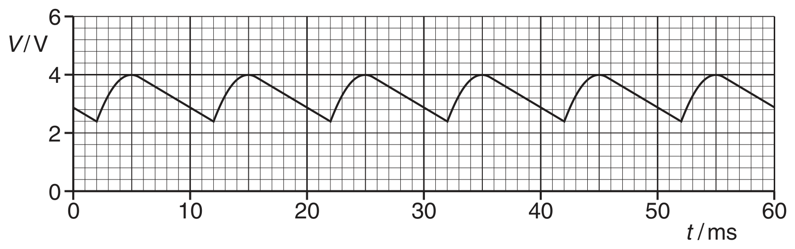
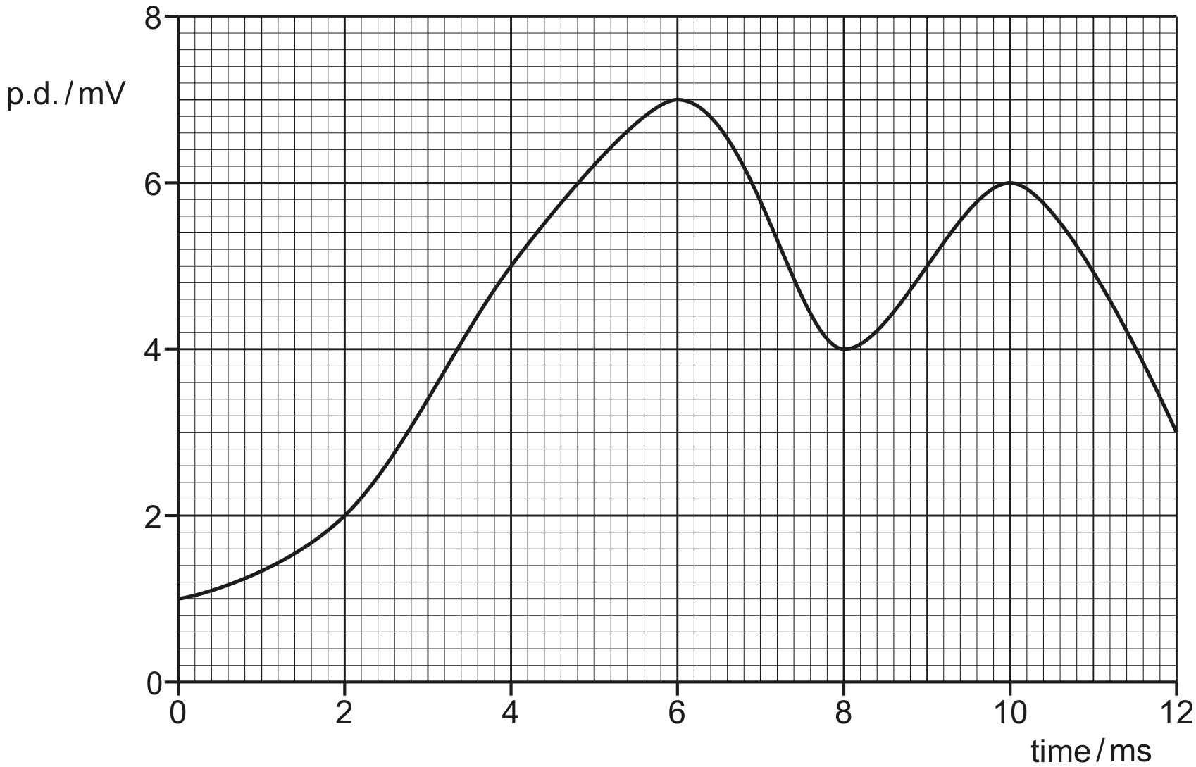
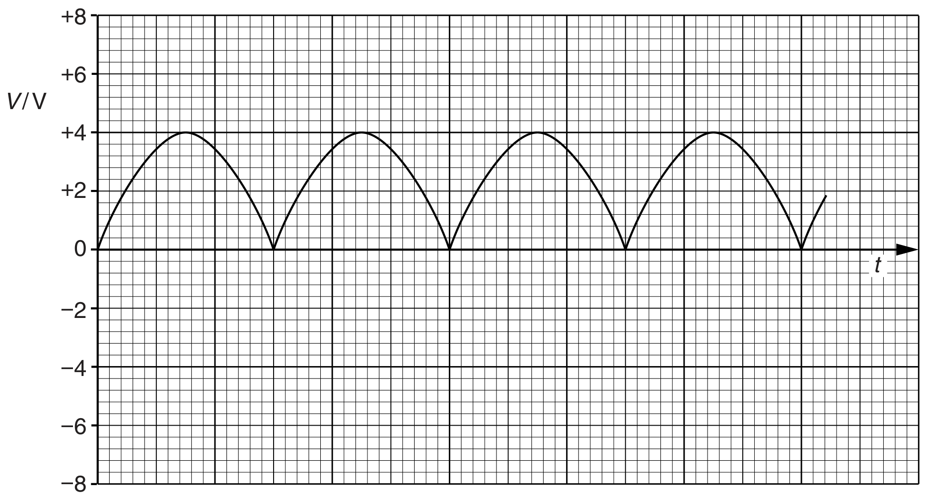
The variation with time t of the p.d. V of the smoothed output is shown in Fig. 4.3.
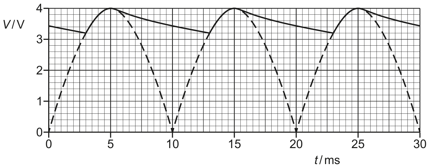
Fig. 4.3

Fig. 4.3

Determine the time constant, in ms , of the smoothing circuit.
time constant = ms

[ 3 ]
[Maximum number: 5]

A sinusoidal alternating voltage supply is connected to a bridge rectifier consisting of four ideal diodes. The output of the rectifier is connected to a resistor R and a capacitor C as shown in Fig. 6.1.

Fig. 6.1

Fig. 6.1

The function of C is to provide some smoothing to the potential difference across R .
The variation with time t of the potential difference V across the resistor R is shown in Fig. 6.2.

Fig. 6.2

Fig. 6.2

(a)

The capacitor C has capacitance 5.0μ F5.0 \mu \mathrm{~F}.

For a single discharge of the capacitor through the resistor R, use Fig. 6.2 to

[ 5 ]
(i)

determine the change in potential difference,

change =V
[ 1 ]
(ii)

determine the change in charge on each plate of the capacitor,

change =

C

[ 2 ]
(iii)

show that the average current in the resistor is 1.1×10³ A1.1 \times 10^{-3} \mathrm{~A}.

[ 2 ]
[Maximum number: 7]

A sinusoidal alternating potential difference (p.d.) from a supply is rectified using a single diode. The variation with time t of the rectified potential difference V is shown in Fig. 5.1.

Fig. 5.1

Fig. 5.1

(a)
(i)

State the type of rectification shown in Fig. 5.1.

[ 1 ]
(b)

The alternating potential difference is rectified and smoothed using the circuit in Fig. 5.2.

Fig. 5.2

Fig. 5.2

The capacitor has capacitance C of 85μ F85 \mu \mathrm{~F} and the resistor has resistance R.
The effect of the capacitor and the resistor is to produce a smoothed output potential difference VOUT V_{\text {OUT }}. The difference between maximum and minimum values of VOUT V_{\text {OUT }} is 2.0 V .

[ 6 ]
(i)

On Fig. 5.1, draw a line to show VOUT V_{\text {OUT }} between times t=1.0 mst=1.0 \mathrm{~ms} and t=5.0 mst=5.0 \mathrm{~ms}.

[ 3 ]
(ii)

Determine the time, in s , for which the capacitor is discharging between times t=1.0 mst=1.0 \mathrm{~ms} and t=5.0 mst=5.0 \mathrm{~ms}.
time = s

[ 1 ]
(iii)

Use your answers in (b)(i) and (b)(ii) to calculate the resistance R.
R= Ω[2]\Omega[2]

[ 2 ]
[Maximum number: 9]

Fig. 5.1 shows four diodes and a load resistor of resistance 1.2kΩ1.2 \mathrm{k} \Omega, connected in a circuit that is used to produce rectification of an alternating voltage.

Fig. 5.1

Fig. 5.1

(a)
(i)

State what is meant by rectification.

[ 1 ]
(ii)

State the type of rectification produced by the circuit in Fig. 5.1.

[ 1 ]
(b)

A sinusoidal alternating voltage VIN V_{\text {IN }} is applied across the input terminals X and Y. The variation with time t of VIN V_{\text {IN }} is given by the equation

VIN =6.0sin25πtV_{\text {IN }}=6.0 \sin 25 \pi t

where VIN V_{\text {IN }} is in volts and t is in seconds.

[ 1 ]
(i)

On Fig. 5.1, label the output terminals P and Q with the appropriate symbols to indicate the polarity of the output voltage VOUT V_{\text {OUT }}.

[ 1 ]
(c)

The output voltage in (b) is smoothed by adding a capacitor to the circuit in Fig. 5.1. The difference between the maximum and minimum values of the smoothed output voltage is 10 % of the peak voltage.

[ 6 ]
(i)

On Fig. 5.1, draw the circuit symbol for a capacitor showing the capacitor correctly connected into the circuit.

[ 1 ]
(ii)

On Fig. 5.2, sketch the variation with t of the smoothed output voltage.

[ 2 ]
(iii)

Calculate the capacitance C of the capacitor.

C=
[ 3 ]
[Maximum number: 5]

An analogue signal is to be transmitted to a receiver. Before transmission, the signal passes through an analogue-to-digital converter (ADC). After transmission it passes through a digital-to-analogue converter (DAC) before finally reaching the receiver, as shown in Fig. 5.1.

Fig. 5.1

Fig. 5.1

(a)

The variation with time of the potential difference (p.d.) of the input signal is shown in Fig. 5.2.

Fig. 5.2

Fig. 5.2

The ADC has a sampling frequency of 250 Hz and uses 4-bit sampling, with the least significant bit corresponding to 1 mV . The signal is first sampled at time 0 , when the sampled bits are 0001.

[ 2 ]
(i)

Part of the signal received by the receiver, after the sampled signal has passed through the DAC, is shown in Fig. 5.3.

Fig. 5.3

Fig. 5.3

On Fig. 5.3, complete the line to show the received signal for time 0 to time 12 ms .

[ 2 ]
(b)

The ADC in (b) is replaced with one that has a sampling frequency of 500 Hz and uses 3-bit sampling, with the least significant bit corresponding to 2 mV .

On Fig. 5.4, sketch the signal that is now received, after passing through the DAC, from time 0 to time 12 ms .

Fig. 5.4

Fig. 5.4

[ 3 ]
(a)

The output of an ideal transformer is connected to a bridge rectifier, as shown in Fig. 6.1.

Fig. 6.1

Fig. 6.1

The input to the transformer is 240 V r.m.s. and the maximum potential difference across the load resistor is 9.0 V .

[ 1 ]
(i)

On Fig. 6.1, mark with the letter P the positive output from the rectifier.

[ 1 ]
(b)

The variation with time t of the potential difference V across the load resistor in (b) is shown in Fig. 6.2.

Fig. 6.2

Fig. 6.2

A capacitor is now connected in parallel with the load resistor to produce some smoothing.

[ 3 ]
(i)

Explain what is meant by smoothing.

[ 1 ]
(ii)

On Fig. 6.2, draw the variation with time t of the smoothed output potential difference.

[ 2 ]
[Maximum number: 5]

A bridge rectifier consists of four ideal diodes A, B, C and D, connected as shown in Fig. 6.1.

Question image

Fig. 6.1
An alternating supply is applied between the terminals X and Y.

(a)
(i)

On Fig. 6.1, label the positive (+) connection to the load resistor R.

[ 1 ]
(ii)

State which diodes are conducting when terminal Y of the supply is positive.
diode and diode

[ 1 ]
(b)

The variation with time t of the potential difference V across the load resistor R is shown in Fig. 6.2.

Fig. 6.2

Fig. 6.2

The load resistor R has resistance 2700Ω2700 \Omega.

[ 1 ]
(i)

On Fig. 6.1, draw the symbol for a capacitor, connected so as to increase the mean power dissipated in the resistor R.

[ 1 ]
(c)

The capacitor in (b)(ii) is now removed from the circuit.

The diode A in Fig. 6.1 stops functioning, so that it now has infinite resistance.
On Fig. 6.2, draw the variation with time t of the new potential difference across the resistor R.

[ 2 ]
[Maximum number: 6]

The components for a bridge rectifier are shown in Fig. 5.1.

(a)

Complete the circuit of Fig. 5.1 by showing the connections of the supply and of the load to the diodes.

[ 2 ]
(b)

Suggest one advantage of the use of a bridge rectifier, rather than a single diode, for the rectification of alternating current.

[ 1 ]
(c)

State

[ 3 ]
(i)

what is meant by smoothing,

[ 1 ]
(ii)

the effect of the value of the capacitance of the smoothing capacitor in relation to smoothing.

[ 2 ]
[Maximum number: 4]

Part of an electric circuit is shown in Fig. 5.1.

Fig. 5.1

Fig. 5.1

The circuit is used to produce half-wave rectification of an alternating voltage of potential difference (p.d.) VIN V_{\text {IN }}.

The output p.d. across the 14kΩ14 \mathrm{k} \Omega resistor is VOUT V_{\text {OUT }}.

(a)
(i)

A component is missing from the circuit of Fig. 5.1.

Complete the circuit diagram in Fig. 5.1 by adding the circuit symbol for the missing component, correctly connected.

[ 1 ]
(ii)

A capacitor C is shown in the circuit of Fig. 5.1.

State the effect on VOUT V_{\text {OUT }} of including the capacitor in the circuit.

[ 1 ]
(b)

The circuit of Fig. 5.1 is modified so that it produces full-wave rectification of an input voltage. Suggest, with a reason, how VOUT V_{\text {OUT }} now varies with time when VIN V_{\text {IN }} is as shown in Fig. 5.2.

[ 2 ]
[Maximum number: 5]

A student is asked to design a circuit by which a direct voltage of peak value 9.0 V is obtained from a 240 V alternating supply. The student uses a transformer that may be considered to be ideal and a bridge rectifier incorporating four ideal diodes.
The partially completed circuit diagram is shown in Fig. 6.1.

Fig. 6.1

Fig. 6.1

(a)

On Fig. 6.1, draw symbols for the four diodes so as to produce the polarity across the load as shown on the diagram.

[ 2 ]
(b)

Calculate the ratio
ratio =

[ 3 ]
0